CPLD - Complex Programmable Logic Devices CPLD - MAX V 440 Macro 74 IOs
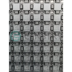


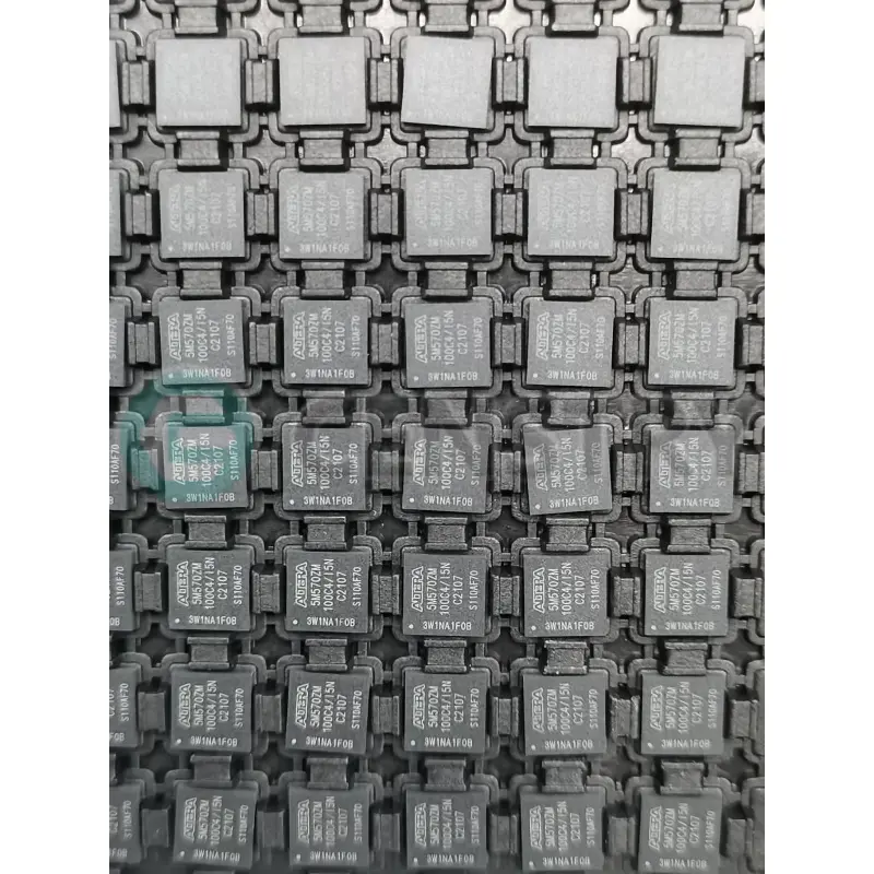
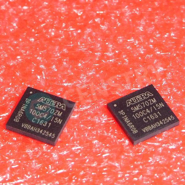
圖片僅供參考.
有關產品詳細信息,請參閱產品規格。
CPLD - Complex Programmable Logic Devices CPLD - MAX V 440 Macro 74 IOs
訂單滿$200即可獲贈限量版中式禮品一份.
訂單金額超過1000 美元可減免30 美元運費.
超過5000 美元的訂單可免運費和交易費.
這些優惠適用於新客戶和現有客戶,有效期為2024年1月1日至2024年12月31日.
Altera
5M570ZM100I5N datasheet
MBGA100
IC芯片
 Lead free/RoHS Compliant
現在提交您的報價請求,我們期望在 7月 02, 2024內提供報價。現在就下訂單,我們期望在 7月 05, 2024內完成交易。時間是格林威治標準時間+8:00。


Feature
The following list summarizes the MAX V device family features:
■ Low-cost, low-power, and non-volatile CPLD architecture
■ Instant-on (0.5 ms or less) configuration time
■ Standby current as low as 25 µA and fast power-down/reset operation
■ Fast propagation delay and clock-to-output times
■ Internal oscillator
■ Emulated RSDS output support with a data rate of up to 200 Mbps
■ Emulated LVDS output support with a data rate of up to 304 Mbps
■ Four global clocks with two clocks available per logic array block (LAB)
■ User flash memory block up to 8 Kbits for non-volatile storage with up to 1000 read/write cycles
■ Single 1.8-V external supply for device core
■ MultiVolt I/O interface supporting 3.3-V, 2.5-V, 1.8-V, 1.5-V, and 1.2-V logic levels
■ Bus-friendly architecture including programmable slew rate, drive strength, bus-hold, and programmable pull-up resistors
■ Schmitt triggers enabling noise tolerant inputs (programmable per pin)
■ I/Os are fully compliant with the PCI-SIG® PCI Local Bus Specification, revision 2.2 for 3.3-V operation
■ Hot-socket compliant
■ Built-in JTAG BST circuitry compliant with IEEE Std. 1149.1-1990
Functional Description
MAX V devices contain a two-dimensional row- and column-based architecture to implement custom logic. Row and column interconnects provide signal interconnects between the logic array blocks (LABs).
Each LAB in the logic array contains 10 logic elements (LEs). An LE is a small unit of logic that provides efficient implementation of user logic functions. LABs are grouped into rows and columns across the device. The MultiTrack interconnect provides fast granular timing delays between LABs. The fast routing between LEs provides minimum timing delay for added levels of logic versus globally routed interconnect structures.
The I/O elements (IOEs) located after the LAB rows and columns around the periphery of the MAX V device feeds the I/O pins. Each IOE contains a bidirectional I/O buffer with several advanced features. I/O pins support Schmitt trigger inputs and various single-ended standards, such as 33-MHz, 32-bit PCI™, and LVTTL.
MAX V devices provide a global clock network. The global clock network consists of four global clock lines that drive throughout the entire device, providing clocks for all resources within the device. You can also use the global clock lines for control signals such as clear, preset, or output enable.

Request a quote 5M570ZM100I5N at censtry.com. All items are new and original with 365 days warranty! The excellent quality
and guaranteed services of 5M570ZM100I5N in stock for sale, check stock quantity and pricing,
view product specifications, and order contact us:sales@censtry.com.
The price and lead time for 5M570ZM100I5N depending on the quantity required, please send your request to us,
our sales team will provide you price and delivery within 24 hours, we sincerely look forward to cooperating with you.
Altera
4000 PCS
EP4CE15E22C8N .PDF
Altera
1 PCS
EP3C16E144I7N .PDF
Altera
2000 PCS
EPM240T100I5N .PDF
Altera
2470 PCS
ES1030QI .PDF
2024-07-01
High quality suppliers.
2024-07-01
CENSTRY offers fast service, good pricing and good parts. Dale, Nick, Steve and Andrew are a true credit to our industry.
2024-06-30
Jen is wonderful and great to deal with
2024-06-29
Censtry is honest, reliable and professional.Great doing business with you. Thank you!
2024-06-27
Maryann Chuang is a nice lady!!! Good telephone phone skills and good attitue.
2024-06-23
Censtry Electronics is a wonderful customer! Jim is the best, very prefessional with fast shipping, hope to work more in the future!
2024-06-15
One of the good companies in China to provide good quality, original parts. always pleasure dealing with mike...
2024-05-30
perfect Sales team with perfect support, thanks
2024-04-28
Professional and reliable company.
2024-02-24
Quick response and on time delivery !


我們高度重視您的回饋意見。 請分享您最真實的評價。
*請在發表評論之前登入您的帳戶